20+ flip flop block diagram
IDM HS committee meetings for 2022 will be held via Microsoft Teams on the following Tuesdays at 12h30-13h30. As one of the inputs on the AND function is Q1 which also acts the output for the whole block.

Clocked T Flip Flop A Characteristic Table B Logic Circuits C Download Scientific Diagram
A dynamical system may be defined formally as a measure-preserving transformation of a measure space the triplet T X Σ μ ΦHere T is a monoid usually the non-negative integers X is a set and X Σ μ is a probability space meaning that Σ is a sigma-algebra on X and μ is a finite measure on X ΣA map Φ.
. Q1 will remember that at some point S1 was true. DD 3 to 20 V and Schmitt trigger buffers with hysteresis equal to 10 of V DD to accept inputs with long rise time. Other MGDs eg IRS210x IRS212x and IRS213x devices have a fixed transition from logic 0 to logic 1 between 15 V to 2 V.
With our money back guarantee our customers have the right to request and get a refund at any stage of their order in case something goes wrong. Half Leather - 0911mm. Many call this a flip-flop function.
The only difference is that the intermediate state is more refined and precise than that of a. In this figure the different functional elements are represented by blocks. Associate member Area of expertise Affiliation.
The notion of cause-and-effect has to be handled carefully when applied to feedback systems. Find a wide range of affordable and stylish furniture online. Block Diagram of Digital Communication System The essential components of a digital communication system are.
For example a 4-bit MISR has a 4-bit parallel output and a 4-bit parallel input. It contains 20 pins which have three-state output. Flip-flop types their Conversion and Applications.
The system can then be said to feed back into itself. But the only difference is that instead of connecting the normal outputs of one stage flip-flop as clock signal for next stage flip-flop connect the complemented outputs of one stage flip-flop as clock signal. 2 to 4 Decoder in Verilog HDL.
Learn all about Function Block Diagram FBD the official PLC programming language described in IEC 61131-3. Negative Edge Triggered D flip flop Circuit Diagram. A J-K flip flop can also be defined as a modification of the S-R flip flop.
20 LED related 3 Light Related 14. In the block diagramQ of RS Flip flop is connected no whereI think it must be connected to the the discharge transistorPlease get it corrected. Seat with Pocket Spring Webbing.
A standard LFSR has a single XOR or XNOR gate where the input of the gate is connected to several taps and the output is connected to the input of the first flip-flop. The block diagram of 3-bit Asynchronous binary down counter is similar to the block diagram of 3-bit Asynchronous binary up counter. SAM L10L11 Family Ultra Low-Power 32-bit Cortex-M23 MCUs with TrustZone Crypto and Enhanced PTC Features Operating Conditions.
A complete tutorial of 555 Timer IC with its block diagram working of SENE 555 TimerPin Configuration and pin out diagram Download 555 data sheet. X X is said to be Σ-measurable if and only if for every σ. Full Adder using Verilog HDL.
Processor CPU is the active part of the computer which does all the work of data manipulation and decision making. Schematic diagram of a modern von Neumann processor where the CPU is denoted by a shaded box -adapted from Maf01. Each flip Flop has different input.
This block diagram includes an audio amplifier bistable flip flop circuit amplifier. CD4013B CMOS Dual D-Type Flip-Flop 1 1 Features 1 Asynchronous Set-Reset Capability Static Flip-Flop Operation Medium-Speed Operation. Input transducer 3Formatter 4.
Block diagram of design requirements. Fig1 shows the basic block diagram of a Digital Communication System. The counter is a digital sequential circuit and here it is a 4 bit counter.
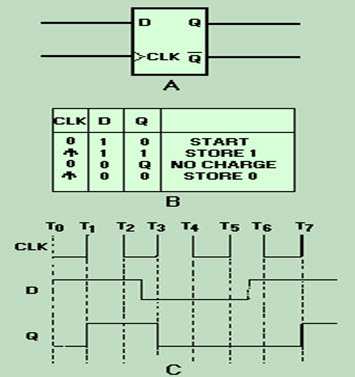
The circuit diagram and truth-table of a J-K flip flop is shown below. The flip flop stores only binary data that has two states are logic 1 and logic 0. S-R Flip-flop Switching Diagram.
162V to 363V -40ºC to 125ºC DC to 32 MHz. A flip flop is an _____ Edge sensitive device Synchronous device Both a and b. In the above block diagram an audio power amplifier is used to amplify audio signals with less power to a level appropriate for controlling loudspeakers.
The set-reset JK delay and trigger or toggle are the most commonly used flip flops. L 880 x W 9401670 x H 5101030 mm. Furniture Mart is the largest online furniture store in Singapore specialising in latest designer furniture Mattresses Bed Frames Wardrobes Sofa Sets for Living room Bed room Dining room and Offices.
Dark Brown or Iceberg. Simple causal reasoning about a feedback system is difficult because the first system influences the. Medical population genomics Genetics Epidemiology Computational risk predication medical OMICS machine learning.
The negative edge D flip-flop can be represented with a triangle and a bubble at the clock end of the D flip-flop block diagram. Some MGDs can drive only one high-side power device eg IRS2117 IRS2127 and IRS21851. 100 nA at 18 V.
Feedback occurs when outputs of a system are routed back as inputs as part of a chain of cause-and-effect that forms a circuit or loop. Block Diagram Working Interfacing. 16 MHz Typical Clock Toggle Rate at 10-V Supply Standardized Symmetrical Output Characteristics Maximum Input Current Of 1-µA at 18 V Over Full Package Temperature Range.
A MISR has the same structure but the input to every flip-flop is fed through an XORXNOR gate. When you press a push button even. All the flip-flops are mainly controllable by the clock and enable pin.
It is worthwhile to further discuss the following components in Figure 41. The result is that the flip-flop looses control of Q and Q and if the two inputs are now switched HIGH again after this condition to logic 1 the flip-flop becomes unstable and switches to an unknown data state based upon the unbalance as shown in the following switching diagram. The working of the clap switch is discussed through the block diagram of the clap switch.

A Simple Bang Bang Loop Using A Flip Flop For A Phase Detector To Lock Download Scientific Diagram
Flip Flop Circuit Types And Its Applications
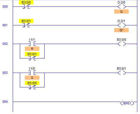
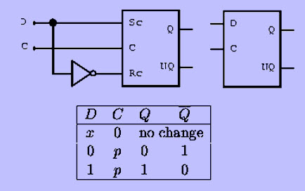
Plc Program To Implement Sr Flip Flop Sanfoundry

Block Diagram Of The Flip Flop Circuit Download Scientific Diagram

Strongarm110 Flip Flop Stable Metastable And Failure Regions Download Scientific Diagram

Quasi Static Negative Edge Triggered D Flip Flop Circuit Layout A Download Scientific Diagram
Test Circuit Schematic For Three Tag Flip Flops Each D Type Flip Flop Download Scientific Diagram
2

A Conceptual Block Diagram Of A Non Volatile Flip Flop And B Download Scientific Diagram

Clocked T Flip Flop A Characteristic Table B Logic Circuits C Download Scientific Diagram

Logic Diagram Of J K Flip Flop Download Scientific Diagram

Measured Output Signal Of The D Flip Flop With Clk And Data Inputs At A Download Scientific Diagram

Cholesterol Distribution In Small Unilamellar Vesicles The Journal Of Physical Chemistry B
Timing Error Aware Microcontroller Springerlink
Timing Error Aware Microcontroller Springerlink

Block Diagram Of The Flip Flop Circuit Download Scientific Diagram
Flip Flop Circuit Types And Its Applications